Semiconductor
High-Resolution Wafer Surface Defect Inspection
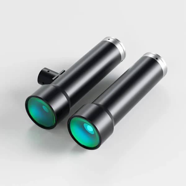
DTCM matrix bi-telecentric lenses with 20MP cameras reliably detect scratches and edge chipping on 12-inch wafers.
01 · Challenge
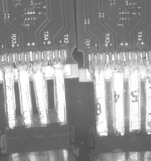
Micron-level scratches imaged inconsistently under conventional lenses due to perspective, causing high false-alarm rates.
02 · Solution
DTCM110's bi-telecentric path removes perspective variation; combined with coaxial illumination, scratch contrast improved more than 3×.
03 · Result
99.7% detection rate, 80% fewer false alarms, 9 seconds per wafer.